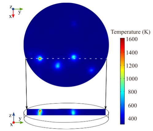
Design and modelling of optical and electronic devices using various numerical technique, including Finite Element Modelling (COMSOL Multiphysics), Finite Difference Time Domain (Lumerical), Rigorous Coupled-Wave Analysis, Ray Tracing (Zemax). Development of bespoke analysis solutions using Matlab and Python. Examples of modelling work can be found in the following articles:
Nanofabrication
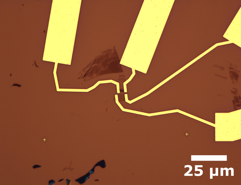
Fabrication of novel devices using a variety of nanopatterning techniques, including Electron Beam Lithography, Optical Lithography, Nanoimprint Lithography. Extensive experience with of thin film deposition techniques (Magnetron Sputtering, Thermal Evaporation, Ion Beam Sputtering) and etching processing (RIE, ICP, IBE, FIB). In depth knowledge of metrology techniques – AFM, SEM, EDX, XRD, Ellipsometry, FTIR. Examples of fabricated devices can be found in the following articles: