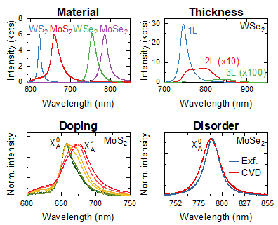
2DMT: Photoluminescence spectroscopy. Part II – μPL setups.

In the first part of this article, we discussed how room-temperature photoluminescence spectroscopy can be used to characterise material properties of atomically-thing transition metal dichalcogenides (TMDs). In Part II, we will focus on experimental setups used for these measurements, describe their main components, and briefly talk about building your own micro-photoluminescence setup.

Figure 1 Examples of micro-photoluminescence setups

Micro-photoluminescence setups (often abbreviated to microPL or μPL) are optical setups designed to measure luminescence spectrum of samples with a very small size (down to or even below few μm) emitted under optical excitation. They can vary substantially in their structure and appearance depending on specific application of this technique (see examples in Fig.1) but will always include four main components:  excitation source, optical system, detector, and sample imaging and positioning system. Let’s discuss these elements in more details.  

2DMT: Photoluminescence spectroscopy. Part I.

In this article, we will discuss the use of room-temperature photoluminescence spectroscopy for the characterisation of material properties of the four most commonly studied semiconducting group-VI transition metal dichalcogenides (TMDs): WS2, MoS2, WSe2, and MoSe2.

We will show how photoluminescence spectroscopy can be used to identify material composition, number of layers, strain, carrier concentration, and disorder level in atomically thin TMD samples. While the accuracy of information extracted from photoluminescence spectra acquired at room temperature is limited by phonon-induced broadening of emission peaks, it can be used for qualitative assessment, providing convenient and accessible way of characterising various material parameters.

2DMT: Optical contrast measurements

  • Optical contrast is a normalised difference between the intensities of light reflected by sample and surrounding substrate
  • Optical contrast of layered materials changes in a step-like manner with increasing number of layers, allowing accurate thickness estimate for flakes up to 15 layers thick
  • Optical contrast measurements work best for materials with strong absorption in the visible range, such as graphene, transition metal mono- and dichalcogenides, deposited onto silicon substrates with 90 or 290 nm dioxide layer, but can be extended to other types of substrates

2DMT: Optical microscopy

  • Optical microscopy is an essential tool in 2D materials research due to the small typical size of the samples.
  • Three most commonly used microscopy methods are bright-field, dark-field, and photoluminescence microscopy.
  • Bright-field microscopy used reflected/transmitted light to produce a magnified image of a sample. Most common applications: flake search (identification of monolayer flakes produced by mechanical exfoliation), thickness measurements through optical contrast measurements, crystal axis direction identification using flake edges.
  • Dark-field microscopy relies on the light scatter by the sample and is used to identify inhomogeneous features, such as trapped contamination and edges/steps in thickness.
  • Photoluminescence microscopy uses light emitted by the sample under optical excitation. While only applicable to luminescent materials, such as monolayer group-VIB transition metal dichalcogenides, it can provide various information about the sample, including thickness, composition, material and interface quality.

2D Materials Toolkit: Introduction

Welcome to 2D Materials Toolkit, a series of articles where we cover key methods used in fabrication, characterisation, and measurement of atomically thin layered materials and their heterostructures. This series is designed for early career researches working with 2D materials, but will also be helpful for more mature scientists and engineers who would like to expand their research into this field. We will focus on practical aspect of different techniques, aiming to give you skills that you can apply in a lab today.

Over the last 8 years of my research career, I was fortunate to be a member of four groups working with 2D materials and collaborate with many more, and I would often find that some things that were considered common knowledge were not so common after all. This discovery went both ways: sometimes I was able to show my colleagues a method that substantially simplified their experiment, other times they helped me find an easy solution to a problem I’d been working on for several months. Perhaps this shouldn’t be surprising, as the field of 2D material research is still very young and rapidly expanding, and there hasn’t been enough time to establish standard fabrication and measurements protocols.

The aim of this series is put together a knowledge base covering the most important methods used in research of atomically thin materials and van der Waals heterostructures. The articles are intended to be quick start guides rather than a comprehensive manuals, giving you essential information to start your own research. We are planning to edit and expand them over time, so make sure to check the revision history at the bottom of the page. We hope you will find this useful, and please do get in touch with any comments or suggestions.

Lightnotes – alpha version

Welcome to the alpha version of Lightnotes.info! We are not sure how you came across our blog, but we are glad to see you here.

The website and blog are both still under construction, which we decided to do live. Stick around to watch our work in progress, or come back few weeks later for our reviews of the most interesting things in the world of nanophotonics.