In this article, we will discuss the use of room-temperature photoluminescence spectroscopy for the characterisation of material properties of the four most commonly studied semiconducting group-VI transition metal dichalcogenides (TMDs): WS2, MoS2, WSe2, and MoSe2.
We will show how photoluminescence spectroscopy can be used to identify material composition, number of layers, strain, carrier concentration, and disorder level in atomically thin TMD samples. While the accuracy of information extracted from photoluminescence spectra acquired at room temperature is limited by phonon-induced broadening of emission peaks, it can be used for qualitative assessment, providing convenient and accessible way of characterising various material parameters.
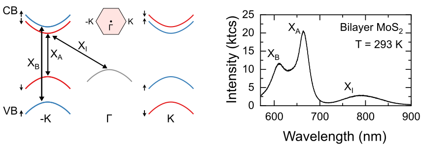
Figure 1 (left) Band-structure of a few-layer transition metal dichalcogenide, showing optical transition giving rise to the most prominent emission peaks in room-temperature photoluminescence spectra. (right) Emission spectrum of a bilayer MoS2 acquired at room temperature, showing emission peaks corresponding to different excitonic species.
Optical properties of atomically thin TMDs are a vast topic that cannot be covered in a short article. We will briefly discuss the key aspects required for the interpretation of room-temperature emission spectrum. For a deeper dive into the topic, we recommend an excellent colloquium by G. Wang et al.
Group IV semiconducting TMDs have direct bandgap only in their monolayer form, with the minimum of the conduction and the maximum of the valence bands located at the -K and K points at the edges of their hexagonal Brillion zone.
Bandgap becomes indirect (typically KC-ΓV) in thicker samples, as hybridisation of states between the layers pushes valence band states at the centre of the Brillion zone up, while the states at the ±K points remain largely unchanged.
Valence band states at -K and K points show spin splitting of ~ 200-400 meV due to the strong spin-orbit interaction in the transition metal atoms. The spin-split bands have the opposite ordering at -K and K points due the lack of in-plane inversion symmetry, leading to effective spin-valley locking. Spin-splitting of conduction band is much weaker (typically 1-40 meV), as they originate from lighter chalcogen atoms.
Excitons (quasi-particles formed by an electron and a hole bound by Coulomb attraction) in TMDs have extremely high binding energies (up to 500 meV, compared to 1-10 meV typical for bulk semiconductors) due to the combination of quantum confinement and lack of dielectric screening from surrounding layers. As a result, optical properties of TMDs are governed by strong excitonic resonances.
Due to the high binding energies, other multi-particle complexes can exist, such as charged excitons (also known as trions), composed of an exciton and an additional charge (electron or hole).
Most prominent peaks in the emission spectrum of TMDs originate from radiative recombination of different excitonic species.
Typical room-temperature emission spectrum of a monolayer TMD consists of a single peak which corresponds to neutral A exciton (X0A), composed of a hole residing at the higher-energy sub-band in valence band and an electron in the conduction sub-band with the same spin at ±K points of the Brillion zone. Emission of B exciton (X0B), composed of a hole in the lower valence sub-band and an electron in the same-spin conduction band, can be present at energies higher than X0A emission energy, although in most materials it has much lower intensity (<1%). MoS2 is one notable exception, where it can be clearly observed, having ~10% intensity of X0A. In samples with high carrier concentration (doping), a charge exciton peak (X*A) can be present, typically visible as a low-energy shoulder of the X0A peak. In addition to these peaks, multi-layer samples also show a low-energy peak (XI) corresponding to the indirect (KC-ΓV) band gap emission which can appear as a separate broad peak or a pronounced lower-energy shoulder of the X0A peak.
Material and thickness identification
Figure 1 (left) Band-structure of a few-layer transition metal dichalcogenide, showing optical transition giving rise to the most prominent emission peaks in room-temperature photoluminescence spectra. (right) Emission spectrum of a bilayer MoS2 acquired at room temperature, showing emission peaks corresponding to different excitonic species.
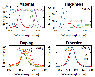
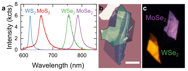
PL spectroscopy provides a fast and convenient method for the identification of materials based on their emission wavelength. Figure 2a compares room-temperature PL spectra recorded in monolayer crystals of four group VI TMDs. Typical peak emission wavelengths for the materials are listed in the table on the right.
Material
Wavelength (Energy)
WS2
620 nm (2.0 eV)
MoS2
660 nm (1.88 eV)
WSe2
750 nm (1.65 eV)
MoSe2
785 nm (1.58 eV)
While peak emission wavelength can be affected by extrinsic effects, including mechanical strain, doping, material thickness, and dielectric environment, the difference in emission wavelength between different materials is sufficiently high for unambiguous identification. The most common application for this method is the identification of material composition in samples containing more than one TMD, such as vertical or lateral heterostructures. Figure 2b shows a bright-field microscope image of a vertical MoSe2/WSe2 heterostructure assembled from mechanically exfoliated flakes using deterministic dry transfer. Although the two materials have very similar appearance, they can be easily distinguished by their emission colour in the wide-field PL image shown in panel c. Monolayer MoSe2 region appears pale pink and monolayer WSe2 has bright yellow colour, reflecting the difference in their emission wavelengths. This method gives the most accurate results when comparing samples which are as similar as possible, i.e. prepared using the same fabrication method and deposited onto the same substrate. In such cases, its application can be extended to TMD alloys, with emission energy changing gradually with sample composition.
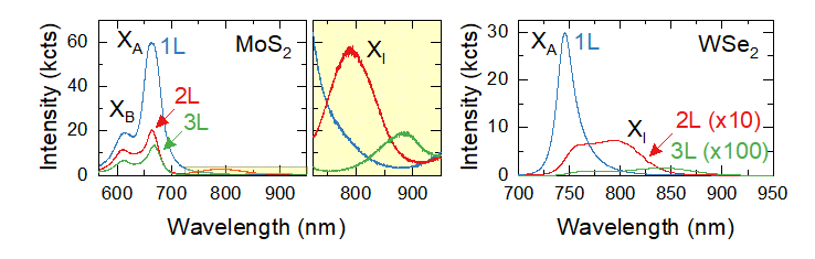
Room-temperature PL spectra of monolayer, bilayer, and trilayer crystals of (left) MoS2 and (right) WSe2.
Changes in the band structure with increasing number of layers lead to a substantial change in the emission spectrum which can be used to identify single- and few-layer flakes. Figure 3 shows emission spectra for MoS2 and WSe2 crystals with thickness ranging from 1 to 3 layers. In monolayer TMDs, the lowest energy transition occurs between the edges of the conduction and valence band at the ±K points. As a result, the emission spectrum of single-layer crystals is characterised by a strong and spectrally narrow emission peak originating from the radiative recombination of neutral A excitons (X0A). In some materials (MoS2 in particular), a weaker B exciton (X0B) peak is visible at higher energy. In bilayer samples, as the maximum of valence band moves to the Γ point at the centre of the Brillouin zone, an additional peak corresponding to indirect band gap emission (XI) appears at lower energy. It is usually well separated from X0A in WS2 and MoS2 but can have a substantial overlap with it in WSe2 and MoSe2. Change from direct to indirect band gap leads to stronger non-radiative recombination and consequently a substantial reduction of the overall PL intensity, although the difference in intensity between a mono- and bilayer depends on other materials parameters and should be used with caution. Further increase in thickness makes the energy difference between direct and indirect bandgap larger – as a result, XI peak moves to lower energy, and overall intensity is further decreased. The change typically becomes negligible after N = 5-7 layers.
Strain and doping level
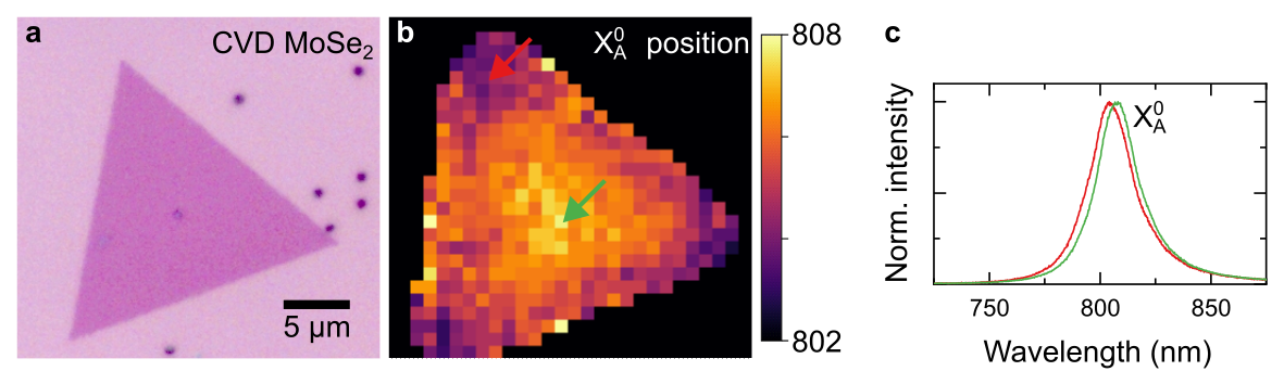
Figure 4 (a) Microscope image of a CVD-grown monolayer MoSe2 on a SiO2/Si substrate. (b) Photoluminescence map of the sample in (a) showing strain-induced variation of neutral exciton peak position (c) Normalised photoluminescence spectra recorded at the locations indicated by colour arrows in panel (b). Lower emission energy of X0 in the centre of the crystal compared to its edge shows higher level of tensile strain.
Two-dimensional crystals produced by both mechanical exfoliation and CVD growth typically show a variation of strain across the sample, which can have a noticeable effect on their properties. For group-VI TMDs, strain leads to a change in the size of their bandgap, which increases for compressive strain and reduces for tensile strain. The position of the neutral exciton peak can therefore be used to estimate the level of strain in the sample: compressive strain leads to a blue-shift of X0A, while tensile strain leads to its red-shift. One of the common examples of intrinsic strain is the one induced in CVD-grown samples during their cooldown from growth to ambient temperature, caused by the mismatch in thermal expansion coefficient between the 2D crystal and the underlying substrate. Figure 4a and b compares a microscope image of a monolayer MoSe2 prepared by CVD growth on SiO2/Si substrate and the map of the X0A position extracted from its room-temperature PL spectra. The latter shows that X0A appears at lower energy (i.e. longer wavelength) in the centre of the crystal compared to its edges, indicating higher level of tensile strain. Strong van der Waals interaction causes MoSe2 crystal to contract by the same amount as the SiO2 substrate during cooldown, despite roughly six times larger thermal expansion coefficient. This results in a sample being tensile strained, i.e. stretched. Edges of the crystal can partially relax this strain, as there is less surrounding material holding them in place.
Photoluminescence shows extremely high sensitivity to strain compared to other spectroscopic signals. For example, in monolayer MoS2 X0A photoluminescence peak shifts by 193 meV for 1% of applied strain, while Raman peak changes only by 0.9 meV, making small changes in strain much easier to detect using photoluminescence spectroscopy. However, changes in X0A position can be caused by effects other than strain, most notably by a change in dielectric environment, so strain analysis using room-temperature photoluminescence spectroscopy works best for samples that are very similar, i.e. produced by the same method and deposited onto the same type of substrate. Even then, it can only be used to compare relative level of strain, while its absolute values can be measured using Raman spectroscopy.
s
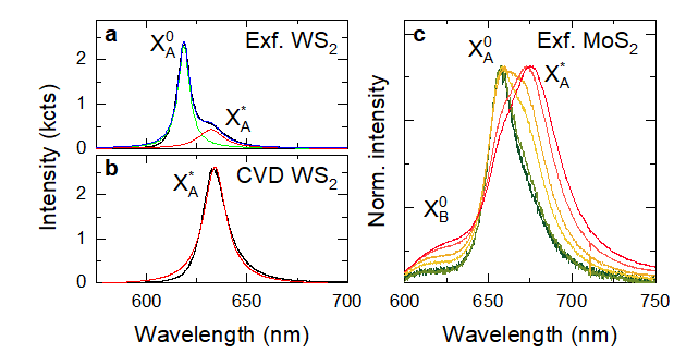
Figure 5 (a and b) Room-temperature photoluminescence spectra of WS2 monolayers produced by (a) mechanical exfoliation and (b) CVD-growth. The exfoliated sample shows emission coming from neutral (X0A) and charger (X*A) exciton peaks. In contrast, emission spectrum of the CVD-grown sample is dominated by X*A emission (c) Normalised photoluminescence spectra of monolayer MoS2 recorded at different excitation powers, ranging from 1 μW (green) to 300 μW (red). Increasing contribution of X*A at higher excitation power is a results of photo-induced doping.
While in bulk semiconductors unbalanced charge carriers typically originate from impurities, in 2D semiconductors high concentration of charge carriers can be created through electrostatic doping, i.e. by injecting them from an electrode using FET-like structure. The term “doping” in the context of 2D materials therefore is commonly used to describe both unbalanced charge carrier population created by defects and impurities, as well as electrostatically induced change in their chemical potential. Neutral excitons can bind to the unbalanced charge carriers, forming a charged exciton, also known as trion. Room temperature photoluminescence peak of charged excitons typically appears ~30 meV below neutral exciton peak and has lower intensity due to a lower binding energy. Figure 5a shows an example of emission spectrum of a mechanically exfoliated monolayer WS2: the main peak at 618 nm corresponds to the neutral exciton (X0A), while the charged exciton peak (X*A) appears as a weaker shoulder at 632 nm. As extrinsic carrier concentration increases, X*A peak becomes more prominent, while the intensity of X0A peak decreases. Therefore, the X*A/X0A intensity ratio can be used to estimate carrier concentration in the sample. At high doping levels, X*A photoluminescence peak can completely dominate the emission spectrum. Figure 5b plot a photoluminescence spectrum recorded in a CVD-grown WS2 sample. Here, high density of sulphur vacancies leads to a very high carrier concentration, resulting in the photoluminescence coming almost exclusively from the X*A peak.
When using X*A/X0A intensity ratio to estimate doping level, measurements should be performed at the lowest laser power possible, as photoexcitation itself can lead to a temporary change in carrier concentration due to photodoping effect. Samples on SiO2/Si substrates are particularly susceptible to photodoping due to photoexcitation of interfacial charge traps in the oxide layer. Figure 5c shows an example of photodoping effect in an exfoliated monolayer MoS2 sample on a SiO2/Si substrate. Curves with different colours correspond to normalised photoluminescence spectra recorded using different excitation power, ranging from 1 μW (green) to 300 μW (red). At lower excitation power, the main feature visible in the photoluminescence spectrum corresponds to the neutral A exciton (X0A), with trion (X*A) emission appearing as a weaker low-energy shoulder. As excitation power is increased, more charge carriers are generated in the silica layer and transferred into MoS2 crystal, leading to a higher relative intensity of X*A emission. Photodoping dissipates when the optical excitation is removed, however, it can take up to several minutes to fully disappear.
a
Material quality and disorder
Presence of disorder, i.e. random variation of material properties on the length scale smaller than excitation spot, leads to broadening of emission peaks, making photoluminescence spectroscopy a powerful tool for studying material quality. It is particularly useful for studying point defects in TMD crystals, as excitons created by photoexcitation ‘funnel’ towards local energy minima, resulting in a disproportionally large part of overall emission coming from these regions.
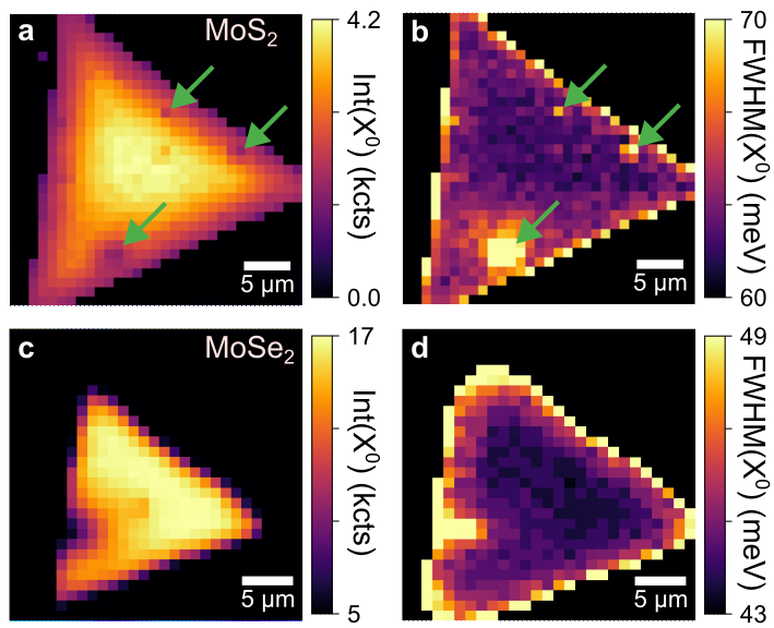
Figure 6 shows photoluminescence maps of MoS2 and MoSe2 crystals produced by CVD growth, plotting intensity (a and c) and position (b and d) of the neutral exciton peak. In both samples, we can see a substantial broadening of the emission peak at the edges of the crystal where defect density is higher. In addition to it, the MoS2 sample shows several areas within the interior of the crystal with increased X0A FWHM, likely corresponding to point defects created during growth. These areas area also visible in photoluminescence intensity maps, as stronger non-radiative recombination enabled by the presence of disorder leads to a reduction of emission intensity.
Figure 6 Photoluminescence maps of CVD-grown MoS2 (top) and MoSe2 (bottom) crystals, plotting intensity (a and c) and FWHM (b and d) of the neutral exciton peak. The presence of disorder leads to the reduction of emission intensity and the broadening of the emission peak. This is typically observed at the edges of the crystals, as well as for some interior regions, such as the ones shown by green arrows in panels (a) and (c).
For quantitative analysis of material quality, photoluminescence measurements need to be performed at cryogenic temperatures to reduce phonon contribution to peak broadening. However, room-temperature FWHM can still give a good qualitative estimate, particularly for samples with higher level of disorder.
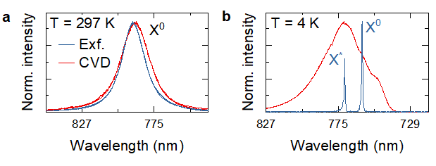
Figure 7 Photoluminescence spectra recorded in exfoliated (blue) and CVD-grown (red) MoSe2 monolayers at room (T = 297 K, a) and cryogenic (T = 4 K, b) temperatures, showing the effect of disorder on the emission spectrum.
Figure 7a compares room-temperature photoluminescence spectra in two MoSe2 samples: blue corresponds to a sample produced by mechanical exfoliation and fully encapsulated in hexagonal boron nitride (hBN), while red shows a sample produced by CVD growth on SiO2/Si substrate. The latter shows a broader linewidth, indicating higher degree of disorder. We can get further insight into the difference between the two samples by fitting their emission peaks with the Voigt function. Lorentzian component of the Voigt function represents homogeneous linewidth which is defined primarily by exciton lifetime and has similar value (~32 meV) in both samples. In contrast, Gaussian component represents inhomogeneous broadening caused by disorder and has much higher FWHM in the CVD-grown sample (~26 meV in the CVD-grown sample compared to ~16 meV in the CVD sample). The difference in the disorder level becomes apparent in the photoluminescence spectra recorder at T = 4K. The emission spectrum of the exfoliated sample shows two sharp peaks corresponding to neutral and charge exciton peaks, with the linewidth of ~1.3 meV, approaching homogeneous limit. In contrast, broadening of photoluminescence peaks combined with strong emission coming from localised exciton states in the CVD grown samples makes individual peaks difficult to discern.
Further reading
“Colloquium: Excitons in atomically thin transition metal dichalcogenides” by G. Wang et al. – an excellent article covering optical properties of monolayer TMDs (Rev. Mod. Phys., arXiv)
“Guide to optical spectroscopy of layered semiconductors” by S. Shree et al. – an in-depth review of optical spectroscopy methods used for characterisation of atomically-thin TMDs and their heterostructure (Nat. Rev. Phys., arXiv)
“Optical Detection of Strain and Doping Inhomogeneities in Single Layer MoS2” – an example of identification of strain and doping in monolayer MoS2 using room-temperature photoluminescence and Raman spectroscopy (Appl. Phys. Lett., arXiv)