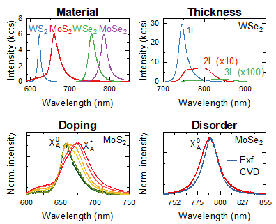
In this article, we will discuss the use of room-temperature photoluminescence spectroscopy for the characterisation of material properties of the four most commonly studied semiconducting group-VI transition metal dichalcogenides (TMDs): WS2, MoS2, WSe2, and MoSe2.
We will show how photoluminescence spectroscopy can be used to identify material composition, number of layers, strain, carrier concentration, and disorder level in atomically thin TMD samples. While the accuracy of information extracted from photoluminescence spectra acquired at room temperature is limited by phonon-induced broadening of emission peaks, it can be used for qualitative assessment, providing convenient and accessible way of characterising various material parameters.
Optical contrast is a normalised difference between the intensities of light reflected by sample and surrounding substrate
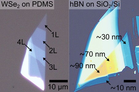
Optical contrast of layered materials changes in a step-like manner with increasing number of layers, allowing accurate thickness estimate for flakes up to 15 layers thick
Optical contrast measurements work best for materials with strong absorption in the visible range, such as graphene, transition metal mono- and dichalcogenides, deposited onto silicon substrates with 90 or 290 nm dioxide layer, but can be extended to other types of substrates
Optical microscopy is an essential tool in 2D materials research due to the small typical size of the samples.
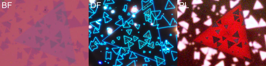
Three most commonly used microscopy methods are bright-field, dark-field, and photoluminescence microscopy.
Bright-field microscopy used reflected/transmitted light to produce a magnified image of a sample. Most common applications: flake search (identification of monolayer flakes produced by mechanical exfoliation), thickness measurements through optical contrast measurements, crystal axis direction identification using flake edges.
Dark-field microscopy relies on the light scatter by the sample and is used to identify inhomogeneous features, such as trapped contamination and edges/steps in thickness.
Photoluminescence microscopy uses light emitted by the sample under optical excitation. While only applicable to luminescent materials, such as monolayer group-VIB transition metal dichalcogenides, it can provide various information about the sample, including thickness, composition, material and interface quality.