- Optical contrast is a normalised difference between the intensities of light reflected by sample and surrounding substrate
- Optical contrast of layered materials changes in a step-like manner with increasing number of layers, allowing accurate thickness estimate for flakes up to 15 layers thick
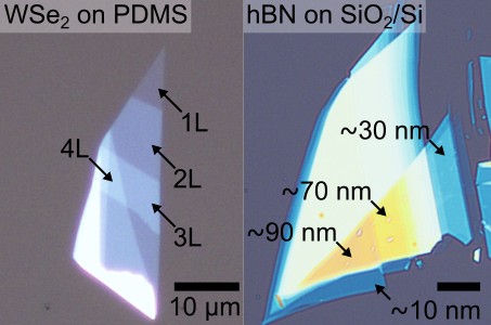
- Optical contrast measurements work best for materials with strong absorption in the visible range, such as graphene, transition metal mono- and dichalcogenides, deposited onto silicon substrates with 90 or 290 nm dioxide layer, but can be extended to other types of substrates
Introduction
It is difficult to overestimate the importance of the optical contrast measurements for the development of the 2D materials research. Together with mechanical exfoliation, it makes the field accessible to a wide variety of research groups around the world and enables rapid fabrication and characterisation of 2D samples. Thickness identification using optical contrast measurements relies on the change of the optical contrast of layered materials with increasing number of layers which occurs in a step-like manner and allows accurate estimate of flake thickness for samples up to 15 layers thick. Optical contrast measurement can be used for samples deposited onto a variety of substrates but give the most accurate results for SiO2/Si with 90 or 290 nm thick silica layer.
Optical contrast
Optical contrast is the normalised difference between the intensities of light reflected by sample and surrounding substrate and is usually defined as C = (Isample – Isubstrate)/ (Isample + Isubstrate), where Isample and Isubstrate are intensities of light reflected by sample and substrate, respectively. Other commonly used definition is C = (Isample – Isubstrate)/ Isubstrate. Physical process which defines the optical contrast will depend on the substrate used for materials deposition, leading to different signs and absolute values.
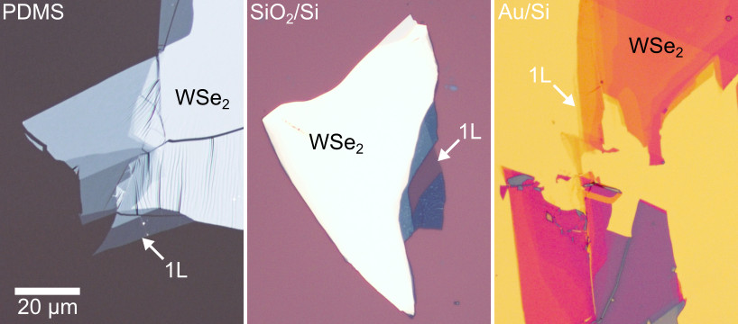
To illustrate this, we can compare optical microscope images of WSe2 flakes deposited onto three different substrates: PDMS, 90 nm SiO2/Si, and gold. Flakes deposited onto PDMS show positive optical contrast, i.e. they appear brighter than surrounding substrate. In case of WSe2 deposited onto SiO2/Si, the contrast is negative for few-layer regions, but becomes positive with increasing thickness. Finally, WSe2 flakes on gold show negative optical contrast and a distinctive change in their colour with increasing thickness. Despite the difference in value and sign of optical contrast, all three samples show a systematic change in their appearance with increasing number of layers, which can be used to identify monolayers and estimate the thickness of few-layer regions.
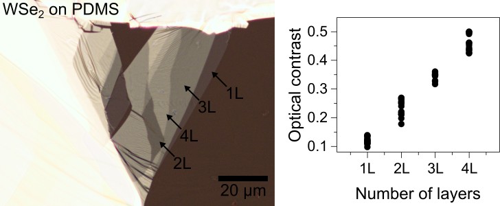
Optical contrast measurements are most commonly used in a qualitative way during flake search to identify monolayers based on their translucent appearance and low optical contrast. An experience user working with a familiar microscope, substrate, and material can identify monolayers with almost 100% accuracy. For more quantitative measurement, optical contrast can be calculated using an image processing software. Figure above shows another example of a WSe2 flake deposited onto PDMS substrate, as well as optical contrast values extracted from mono- and few-layer regions of eight different samples. Even though the contrast values for each thickness show random fluctuations caused by variation of acquisition parameters and non-uniform illumination, the difference between adjacent thicknesses is sufficiently high to accurately estimate the number of layers in each region. Moreover, this difference (around 0.11 for the samples shown above) is equal to the optical contrast of a monolayer region – this allows you to estimate the expected value for a single layer region even before you find one.
Step-by-step guide
Optical contrast is calculated by measuring the intensity of three colour channel (red, green, and blue) in the digital colour image. It can be done using different software, but one of the most convenient choices is ImageJ, a free and power software for microscope image processing.
- Acquire an image of the flake, making sure that it is properly focused and exposed
- Save the image as a high-quality file (tiff or jpeg with at least 90% quality)
- Open the acquired imaged in ImageJ by using the file menu or by dragging and dropping the file onto ImageJ window
- Use circular selection tool to select an area of your flake. Press M to perform intensity measurements.
- Use mouse to drag the selection onto the substrate, keeping the minimum distance between the measurement points, and repeat the measurements.
- Calculate the optical contrast as C = (Isample – Isubstrate)/ (Isample + Isubstrate)
- Repeat the measurements for regions with different thickness to estimate the optical contrast expected for monolayer from the minimal difference between adjacent thicknesses.
- Calculate the number of layers in the selected region by dividing its optical contrast by the expected monolayer contrast.
Troubleshooting
- Make sure that white balance is set correctly – use a piece of white paper to set it.
- Save you images with sufficiently high quality (tiff, jpeg with >90% quality)
- Keep the distance between the measurement spots to a minimum
- Make sure none of the colour channel are underexposed or clipping
- Different optical systems (e.g. microscope lenses, light source, cameras) will provide different contrast – if you are comparing results of different measurements, make sure they were taken using the same system.
- Optical contrast can also be affected by acquisition setting (sensitivity, exposure time, WL intensity)
- For increases accuracy, consider calculating optical contrast for individual colour channels
- If your camera is noisy, take a reference image and subtract the noise background prior to optical contrast calculations
- Use another method (AFM, Raman or PL) to verify measurement results
Further reading
- “Rapid and Reliable Thickness Identification of Two-Dimensional Nanosheets Using Optical Microscopy” by H. Li et al. – Identification of thickness for different layered materials up to 15 layers thick deposited onto SiO2/Si substrate with 90 or 300 nm dioxide layer thickness using optical contrast measurements (ACS Nano, arXiv)
- “Viscoelastic Transfer of 2D Material Using PDMS” – our detailed text and video guide to 2D material preparation and transfer made in collaboration with Osilla, which includes thickness identification using optical contrast measurements (Osilla website).
- “Broad range thickness identification of hexagonal boron nitride by colors” by Y. Anzai – Identification of hBN thickness using its colour for flakes deposited onto 90 nm SiO2/Si substrates (Applied Physics Express)