- Optical microscopy is an essential tool in 2D materials research due to the small typical size of the samples.
- Three most commonly used microscopy methods are bright-field, dark-field, and photoluminescence microscopy.
- Bright-field microscopy used reflected/transmitted light to produce a magnified image of a sample. Most common applications: flake search (identification of monolayer flakes produced by mechanical exfoliation), thickness measurements through optical contrast measurements, crystal axis direction identification using flake edges.
- Dark-field microscopy relies on the light scatter by the sample and is used to identify inhomogeneous features, such as trapped contamination and edges/steps in thickness.
- Photoluminescence microscopy uses light emitted by the sample under optical excitation. While only applicable to luminescent materials, such as monolayer group-VIB transition metal dichalcogenides, it can provide various information about the sample, including thickness, composition, material and interface quality.
Introduction
In the first article of our 2D Materials Toolkit series, we will discuss optical microscopy, one of the most widely used tools in 2D material research. Despite being less sophisticated than other methods, it finds its application in almost all stages of fabrication and characterisation and is largely responsible for the rapid expansion of the research field, providing an accessible and convenient method for identifying monolayer crystal produced by mechanical exfoliation. We will discuss bright-field, dark-field and photoluminescence microscopy and their application for 2D materials characterisation, including identification of thickness, material composition, crystal axis orientation, and quality of the interlayer interface.
It is important to note that optical schemes we use in this article are simplified for the sake of clarity. For a detailed description of optical schemes used for different imaging techniques, we recommend a great review article “Optical microscopy” by M. W. Davidson and M. Abramowitz
Bright-field microscopy
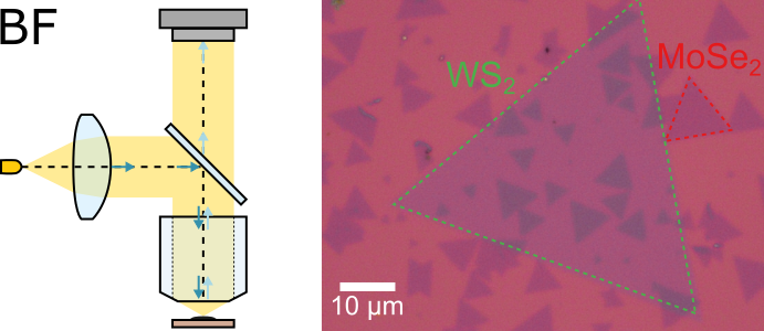
Bright-field (BF) microscopy is the simplest and most commonly used type of optical microscopy. The main application of BF microscopy is creating a magnified image of a sample with appearance similar to what you would see with the naked eye. The most basic form of a BF microscope is a magnifying glass, although research-grade compound microscopes have a much more complex structure to allow higher magnification and better contrast and resolution. A simplified schematics of a BF optical microscope is shown in the figure above: a collimated beam of white light, usually generated by an LED or a halogen lamp, is focused onto a sample using a microscope objective. The light reflected by the sample is collected by the same objective and guided to a camera to form a magnified image. Contrast of the image is defined by the change in the intensity and colour (i.e. combination and relative intensities of wavelengths) of light reflected by different parts of the sample.
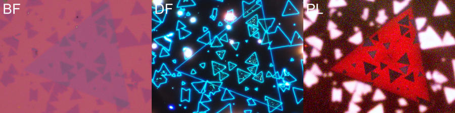
Right panel of the figure shows an example BF image of single-layer MoSe2 and WS2 crystals produced by chemical vapour deposition (CVD) and deposited onto a silicon substrate coated with 290 nm thick layer of silicon dioxide (SiO2). Transition metal dichalcogenide (TMD) crystals appear darker than surrounding SiO2/Si as they reflect less light compared to the bare substrate. The slight difference in colour between WS2 and MoSe2 reflects the difference in their absorption spectra.
The optical setup described above is knows as epi illumination or reflected light microscopy and is the most commonly used scheme as it allows imaging of 2D samples deposited onto non-transparent substrates, such as ubiquitously used SiO2/Si substrates, and provides better optical contrast for atomically thin samples. Trans-illumination, or transmitted light microscopy, uses a condenser lens positioned on the opposite side of the sample to provide illumination and is only applicable for samples on transparent substrates, such as glass, sapphire, or quartz.
Due to the small typical size of 2D crystals (10-100 μm lateral size), BF microscopy is used on all fabrication and characterisation steps where sample need to be located and viewed. As a result, simple custom-built BF microscopes can be found in almost all setups, and it is also not uncommon for setups to be built around a commercial BF microscope. One of the most common application of BF microscopy, at least in term of the total time spent, is flake search, i.e. identification of single- and few-layer crystals (commonly referred to as “flakes”) produced my mechanical exfoliation. Unlike CVD growth which allows thickness of the grown material to be controlled, the majority of material produced by mechanical exfoliation will have thickness of 100s of layers and more, and atomically thin flakes need to be located by visually inspecting the entire substrate. Single- and few-layer crystals can be identified by their low optical contrast and translucent appearance with a remarkably high degree of accuracy, although it will strongly depend on material, substrate, and optical system used. A more quantitative approach relies on optical contrast measurements, i.e. comparing the intensity of light reflected by sample and bare substrate, and can provide accurate thickness identification for up to 10 layers.
BF microscopy images can also be used to identify crystal axes orientation due to the cleavage and growth behaviour of layered crystals with hexagonal lattice. For example, for monolayer TMD flakes produced by CVD growth, the edges of equilateral triangular flakes correspond to zig-zag direction. Similar approach can be used for exfoliated material, as bulk layer crystals tend to cleave primarily along zig-zag direction.
We will cover optical contrast measurements and crystal axis identification for CVD-grown and exfoliated flakes in up-coming articles – stay tuned!
Dark-field microscopy

Dark-field (DF) microscopy is used to create high-contrast images using light scattered by the sample. Samples are usually illuminated at an acute angle with respect to their surface, and back-reflected light (traveling along the same path in reverse direction) is blocked by an aperture, with only scattered light (changing its propagation direction due to interaction with the sample) detected by the camera. As a result, only features that can strongly scatter light (such as flake edges, steps in thickness, and contamination particles) are visible in DF images, appearing as appearing as bright dots and lines on a black background.
DF microscope objectives working with epi illumination are composed of two concentric lens systems: the outer set consisting of ring-shaped lenses is used to illuminate the sample, while the inner set is used to collect the scattered light and form the image. DF-capable objectives can be used for both DF and BF imaging, with the type of illumination defined by the set of optics and beam stops used in the beam splitter. While these objectives are generally quite expensive, a simple DF imaging setup can be created using an external light source.
Right panel of the figure above shows a DF image of the sample presented in the previous image. Uniform regions of both MoSe2 and WS2 appear black in the image as they do not scatter the incoming light. The features visible in the image correspond to points of inhomogeneity, such as edges of flakes, wrinkles formed during transfer, and pockets of contamination trapped between the layers. The ability of DF microscopy to visualise these features make it very valuable for sample inspection on different stages of fabrication. DF images are commonly used to inspect hexagonal boron nitride flakes used for encapsulation to ensure that regions selected for material transfer do not contain steps in thickness or residues, which are usually undetectable in BF images. Another common application for DF microscopy is inspection of interface quality in vertical van der Waals stacks. Strong interaction between different layers can lead to aggregation of residues trapped between them into small pocket in the process known as self-cleaning. An example of such residue pocket can be seen in the image above, clearly visible in the DF image. Overall high contrast and somewhat selective nature of DF imaging make it useful whenever crystal edges need to detected, e.g. for identification of individual 2D crystals embedded into multi-layer van der Waals heterostructure.
Photoluminescence microscopy
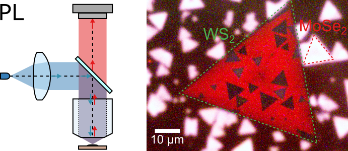
Unlike BF and DF imaging which use light provided by the white-light source for imaging, in case of photoluminescence (PL) microscopy the image is formed by the light emitted by the sample itself, with incident light acting as an excitation source. The PL microscopy therefore is only applicable to the samples which are luminescent. In case of layered 2D materials, it is applied primarily to monolayer and bilayer TMDs with emission peaks in the visible and near-infrared range, i.e. WS2, MoS2, WSe2, and MoSe2.
PL microscopy has the same operating principle as fluorescence microscopy, which is commonly used in biological research. High energy light produced by the light source is absorbed by the sample, causing it to emit light of a lower energy. This light is substantially weaker than reflected excitation light and need to be separated using a long-pass filter and/or dichroic mirror. Unlike fluorescence microscopy which usually requires a dedicated UV source and uses narrow-band emission filters designed a specific fluorophore, PL microscopy of atomically thin TMDs can be achieved by performing a set of simple modifications to an existing BF microscope: First, the emission spectrum of the white-light source should be limited to a higher (blue-green) energy range using a short-pass optical filter. Secondly, and appropriate optical filter (band-pass or long-pass) needs to be introduced to the detection path to block reflected light and isolate weak low-energy PL signal coming from the sample. The use of long-pass filter and colour-sensitive camera allows different materials to be imaged at the same time, with the different emission wavelength appearing as different colours in the image.
The difference between MoSe2 and WS2 PL is clearly visible in the PL image presented above: WS2 has a PL peak at 630 nm which appears as dark red colour. In contrast, MoSe2 emission maximum lies in the near-infrared range at 780 nm and is detected as bright pink by the camera. These colours are defined by the combination of emission spectrum of a material and transmission bands of red, green, and blue filters in the Bayer filter array of the camera. The regions where the two materials overlap appear dark in the PL image is emission in both materials is quenched due to charge transfer between the layers.
PL microscopy is a very power characterisation tool for group VIB TMDs, capable of providing various information about the sample. Single layer TMD flakes can be identified by their bright PL signal, as emission is strongly quenched in bilayers due to direct-to-indirect bandgap transition, and becomes undetectable in trilayers and thicker samples. Individual materials can be selectively imaged by replacing the long-pass filter in detected with a band-pass filter centred at their emission maximum. PL images can be used to quickly identify quality of the sample by inspecting emission intensity and uniformity across the flake area. Finally, the quenching of PL in heterostructure formed by different TMDs can be used to estimate interface quality, as presence of contamination will lead to suppressed interlayer charge transfer.
Further reading
- “Optical Microscopy” by Michael W. Davidson and Mortimer Abramowitz – a comprehensive review article, describing different optical microscopy methods (Olympus website – open access)
- “Rapid and Reliable Thickness Identification of Two-Dimensional Nanosheets Using Optical Microscopy” by H. Li et al – thickness identification in different layered materials up to 15 layers thick using optical contrast measurements (ACS Nano, arXiv)
- “Distinctive in-Plane Cleavage Behaviors of Two-Dimensional Layered Materials” by Y. Gao et al. – identification of crystal axes direction in layered materials with hexagonal lattice using flake edges. (ACS nano -open access)
- “Imaging of Interlayer Coupling in van der Waals Heterostructures Using a Bright-Field Optical Microscope” by E. Alexeev et al. – our paper describing how PL imaging can be achieved using a modified bright-field microscope and discussing some of its applications (Nano letters, arXiv)