In the first part of this article, we discussed how room-temperature photoluminescence spectroscopy can be used to characterise material properties of atomically-thing transition metal dichalcogenides (TMDs). In Part II, we will focus on experimental setups used for these measurements, describe their main components, and briefly talk about building your own micro-photoluminescence setup.
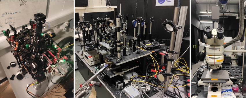
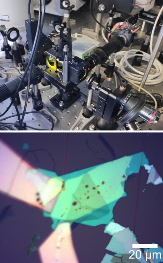
Figure 1 Examples of micro-photoluminescence setups
Micro-photoluminescence setups (often abbreviated to microPL or μPL) are optical setups designed to measure luminescence spectrum of samples with a very small size (down to or even below few μm) emitted under optical excitation. They can vary substantially in their structure and appearance depending on specific application of this technique (see examples in Fig.1) but will always include four main components: excitation source, optical system, detector, and sample imaging and positioning system. Let’s discuss these elements in more details.
Disclaimer: If you are reading this article, we don’t need to tell you that lasers can be extremely dangerous. The information on this website is for general purposes only – use it at your own risk.
Excitation source
With a few notable exceptions, photoluminescence measurements are performed using lasers as excitation source. The are two key parameters that you need to consider when choosing one for your measurements: excitation energy and excitation power. Excitation energy must be sufficiently high to excite material above its band gap and well spectrally separated from its photoluminescence signal so the latter can be isolated using edge-pass or band-pass filters. Common choices for room-temperature spectroscopy of atomically thin TMDs are 532 nm diode-pumped solid state (DPSS) lasers and 520 nm diode lasers: both can be used to excite the six most widely studied group-VI TMDs (WS2, MoS2, WSe2, MoSe2, WTe2, MoTe2), are readily available and relatively inexpensive.
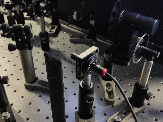
Figure 2 Thorlabs PL202 635 nm laser module used for basic photoluminescence spectroscopy.
Typical excitation powers required for room-temperature photoluminescence spectroscopy range from 1.3∙107 to 2.5∙108 W/m2, which correspond to 10-200 μW focused into a spot with 1 μm diameter. Excitation power higher than 6.4∙ 108 W/m2 (500 μW) can lead to photo-induced damage. Taking into account losses in the optical system, the output power of the laser needs to be higher than 1 mW, thus putting these lasers firmly into class-III category. However, lower-power class-II alignment lasers (such as Thorlabs PL201 520 nm Compact Laser Module) can be used for basic characterisation of monolayer TMDs, as long as the optical system is design accordingly.
Optical system
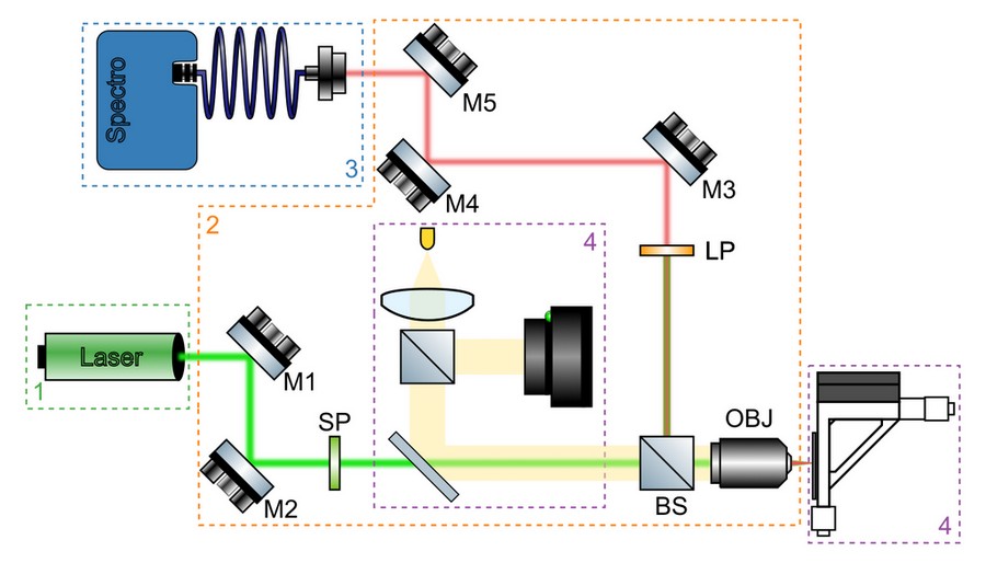
Figure 3 Schematic of a typical micro-photoluminescence setup. Colour rectangles indicate four main components: (1) excitation source, (2) optical system, (3) detector, and (4) sample imaging and positioning system.
A simplified schematics of a micro-PL setup, including all main components, is shown in Figure 3. The purpose of the optical system is to focus excitation light into a tight spot on the sample, collect emitted photoluminescence signal, separate it from the reflected light, and guide it towards the detector. A typical optical system will include the following components:
Excitation path mirrors (M1 and M2)
These mirrors are used to align the incoming laser light, so it enters back aperture of the microscope objective (OBJ) at its centre and traveling parallel to its optical axis. A minimum of two adjustable mirrors is required for this, much in the same way as two points are required to define a line in a 3D space.
Beam splitter (BS)
In reflected-light geometry (also known as epi illumination), same microscope objective is used to focus excitation light on a very small area (typical diameter of 1 μm) and collect photoluminescence emitted by the sample that is propagating in the opposite direction. Excitation and detection beam paths are combined and separated using a beam splitter. A dichroic beam splitter, transmitting light of shorter wavelengths and reflecting longer ones, is used for basic spectroscopy with single excitation source. It is particularly useful for microPL setups with low power excitation sources, as it allows more laser light to be sent to the sample without compromising signal collection efficiency. A more complex measurements, e.g. with multiple excitation sources or polarisation-resolved excitation and detection, typically require an achromatic beam splitter. In this case, a portion of laser light reflected off the beam splitter and photoluminescence signal transmitted through it are lost.
Microscope objective (OBJ)
2D crystals produced by both mechanical exfoliation and CVD growth have typical lateral size of <100 μm and require optical system with high magnification to focus excitation light onto the area of interest on the sample. A minimum of 40x magnification objective is required for most measurements.Microscope objectives with high numerical aperture and magnification will focus laser light to a tighter spot, increasing excitation power density and collecting larger portion of photoluminescence emitted by the sample. For non-planar samples or samples mounted in environmental chambers, an objective with long working distance (i.e. minimum distance between the focal plane and the front element of the objective) is required.
Spectral filters (LP)
Photoluminescence signal produces by the sample is much weaker than reflected excitation light and has to be separated from it using an appropriate long-pass (LP) filter with minimum 4 OD suppression. A dichroic mirror on its own is not sufficient to suppress reflected laser light. If excitation source has additional modes or fluorescent background at lower energy, an additional short-pass filter (SP) or band-pass filter centred at the main mode might be required to suppress them.
Detection path mirrors (M3 and M4)
Similar to excitation path, a minimum of two mirrors is required to guide and align photoluminescence signal collected by the microscope objective to aperture of the detector. The latter is typically a lens which either couples light into a fibre or projects an image of the sample onto the entrance slit of a spectrometer for fibre-coupled or free-spaced spectrometers, respectively.
Detector
Advanced PL spectroscopy requires the use of modular spectrometers with interchangeable gratings and an actively cooled CCD detector to achieve high sensitivity and spectral resolution. These spectrometers can be quite expensive, with typical prices starting at £40,000 even for a basic configuration. However, for basic room-temperature characterization, much cheaper USB-powered fibre-coupled spectrometers can be used, such as those from Ocean Optics, Thorlabs, or Osilla. Thanks to their small size, these spectrometers can be easily integrated into fabrication setups, enabling in-situ sample characterisation. Models equipped with thermoelectrically cooled CCD detectors offer better signal-to-noise, allowing samples with weaker emission (e.g. CVD-grown MoS2) to be studied.
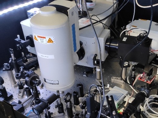
Figure 4 Modular imaging spectrometer with liquid nitrogen cooled CCD (iHR550 and Symphony II, Horiba)
Positioning and imaging system
Sample imaging and positioning systems are an essential part of any 2D characterisation setup. These systems are used to locate the desired crystal on a substrate and focus excitation light on a specific region of interest. For many spectroscopic setups, imaging system is also used for fine-tuning of laser alignment. Figure 5 shows an example of a bright-field imaging system embedded into a microPL setup. It consists of an LED light source, a CMOS camera, and a set of two beam splitters and utilises the same high-magnification microscope objective that is used for PL spectroscopy. Image quality in such simple, custom-built setups is typically lower that the one achieved in commercial bright-field microscopes, but it is more than sufficient for most applications.
Requirements for positioning system are more stringent: it needs to have ~1 μm precision for lateral movement to align excitation spot to a specific region on the sample and better than 1 μm precision for vertical movement to put the sample surface in the focal plane of the microscope objective. Although basic characterisation can be performed using manual stages, motorised positioners can greatly extend system capabilities by allowing you to acquire spectrally resolved PL maps.
Figure 5 (top) Custom-built wide-field imaging system embedded into a microPL setup. (bottom) Image of a van-der Waals heterostructure acquired using the system shown above.
Finding a μPL setup
Room-temperature microPL setups are among the simplest and most inexpensive optical spectroscopy systems, however, we do not recommend trying to build your own if you don’t have prior experience in this area. A better option in this case would be to find a commercial setup that can be adapted or directly used for microPL spectroscopy.
Confocal microscopes.
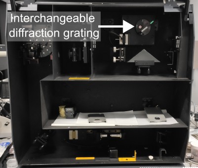
The most common setups that can be used for microPL spectroscopy are confocal Raman microscopes. These systems are designed to measure spectrally narrow signals appearing very close to the excitation laser wavelength and are commonly used in chemistry, biology, and material science. To use them for PL spectroscopy, you will need to change diffraction grating to the one with a lower number of grooves per mm to give you a larger spectral detection window. In some systems (like Horiba Labra HR800), this is done using a motorised grating turret, allowing seamless switching between PL and Raman spectroscopy modes. In others, like Renishaw inVia or RM1000, you will need to gain access to the spectrometer cavity to manually change the grating. Note that dedicated Raman microscopes with fixed grating position cannot be use for PL spectroscopy, as they can only measure signals in a narrow spectral window close to the excitation laser.
Figure 6 Interchangeable grating in Renishaw RM1000 Raman microscope
Another common system that can be adapted for microPL spectroscopy is biological confocal microscopes. These systems are used to image biological samples by scanning laser spot across it and detecting integrated PL intensity as a function of position. Adapting these systems for PL spectroscopy will require changing single-channel detector (typically photomultiplier tube or avalanche photodiode) for a multi-channel one (i.e., spectrometer), as well as changing spectral filters in fluorescence filter cube to enable broadband detection.
Wide-field microscopes
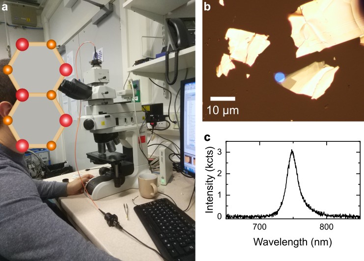
Figure 7 (a) Bright-field optical microscope converted for PL imaging and spectroscopy (b) Detection area of the spectrometer visualised by back-propagating white light through detection fibre. (c) PL spectrum of a monolayer WSe2 acquired using this setup.
If you don’t have access to a commercial confocal microscope that can be used for PL spectroscopy, you can make your own by adding spectrally resolved readout to a wide-field optical microscope that has been modified for PL imaging. A detailed instruction on coupling a spectrometer to an optical microscope can be found in this great work from Andres Castellanos-Gomez group. Figure 7a is a photograph of a Nikon Eclipse LV150N microscope that I modified following this approach. In this case, I connected multi-mode optical fibre to the trinocular port of the microscope and moved the camera to an additional camera port on a Y-IDP Double Port unit with removable 55/45 beam splitter. This way entire photoluminescence signal can be sent to spectrometer, or half of it can be diverted to camera, enabling simultaneous PL imaging and spectroscopy. This arrangement greatly simplifies system alignment, as it allows you to position and focus collection spot by back propagating light from an LED light source through the fibre, as demonstrated in Figure 7a and b.
The microscope has already been modified for wide-field PL imaging using built-in white light source: I have added a 550 nm short-pass and a 600 nm long-pass filters to excitation and detection paths, respectively, and a 550 nm long-pass dichroic mirror to combine and separate them. Figure 7c shows PL spectrum of a monolayer WSe2 collected using this setup and Ocean Optics Flame-S-VIS-NIR spectrometer. Combining bright-field and PL imaging with PL spectroscopy in a single setup makes it an extremely useful tool for rapid characterisation of sample thickness and quality, particularly for crystals produced by mechanical exfoliation.
Further reading
“Micro-reflectance and transmittance spectroscopy: a versatile and powerful tool to characterize 2D materials” – a detailed instruction on how to couple a USB spectrometer to an wide-field optical microscope to enable reflectance contrast measurements (J. Phys. D. Appl. Phys, arXiv)
“Imaging of Interlayer Coupling in van der Waals Heterostructures Using a Bright-Field Optical Microscope” – our paper describing how to convert a bright-field optical microscope for photoluminescence imaging of atomically thin TMDs (Nano Lett., arXiV)
“Guide to optical spectroscopy of layered semiconductors” by S. Shree et al. – a paper reviewing optical spectroscopy methods which includes a detailed description of a low-temperature μPL setup (Nat. Rev. Phys., arXiv)